- A hands-on build of the Game Bub from GitHub, sharing the messy, real process instead of sponsor-polished shortcuts
- Detailed walkthrough of PCB, shell, and firmware, with time sinks like KiCad plugins and manufacturer file generation
- Practical parts advice: battery polarity warning, speaker fit, 3D-printed shell material trade-offs, and glass alternatives
As I was saying in the article, I kicked off a pretty ambitious project — one that had been sitting on my to‑do list for over a year. Why? Because I like projects where you can see someone poured passion into them, where there’s real work behind the result. The opposite of far too much of today’s internet content: influencer fluff and short videos that feel made for people with zero patience.
Like many things that happen unexpectedly, I finally dug it out — with a negative kind of inspiration — after watching another piece of content. I am tired of seeing people on the internet doing something only when there’s a sponsor paying for it, shot cinematically and edited to perfection so everything looks easy, as if there’s a whole team behind it. Reality is different. Real life is messier, and getting to a result means a lot of work, a lot of details, and money that doesn’t come from sponsorships.
This is my real journey, the one anyone will probably go through if they want to build a Game Bub from the project’s source files on GitHub.
With a technical background, I’ve got a bit of everything: hardware, software, programming, electronics, CPU architecture, soldering components. The starting toolkit was generous, and it was still tricky in some places. Honestly though, the project hooked me — so much that I started modifying it, planning new features. But that’s a story for another time.
Because I wanted to pack in as many details as possible, I initially planned to split this into several articles. In the end I decided to keep it as one. It’s longer, but more useful if you follow it from start to finish.
At the end of the article, you’ll find a realistic comparison between building it yourself and buying it ready‑made — strictly from a cost perspective.
What’s in the project
After downloading the project from GitHub, the first step was to get a high‑level view of what’s there. The structure has three major sections:
- The PCB and its components
- The shell, buttons, and mechanical parts
- The firmware
KiCad, Gerbers, and the plugin trap
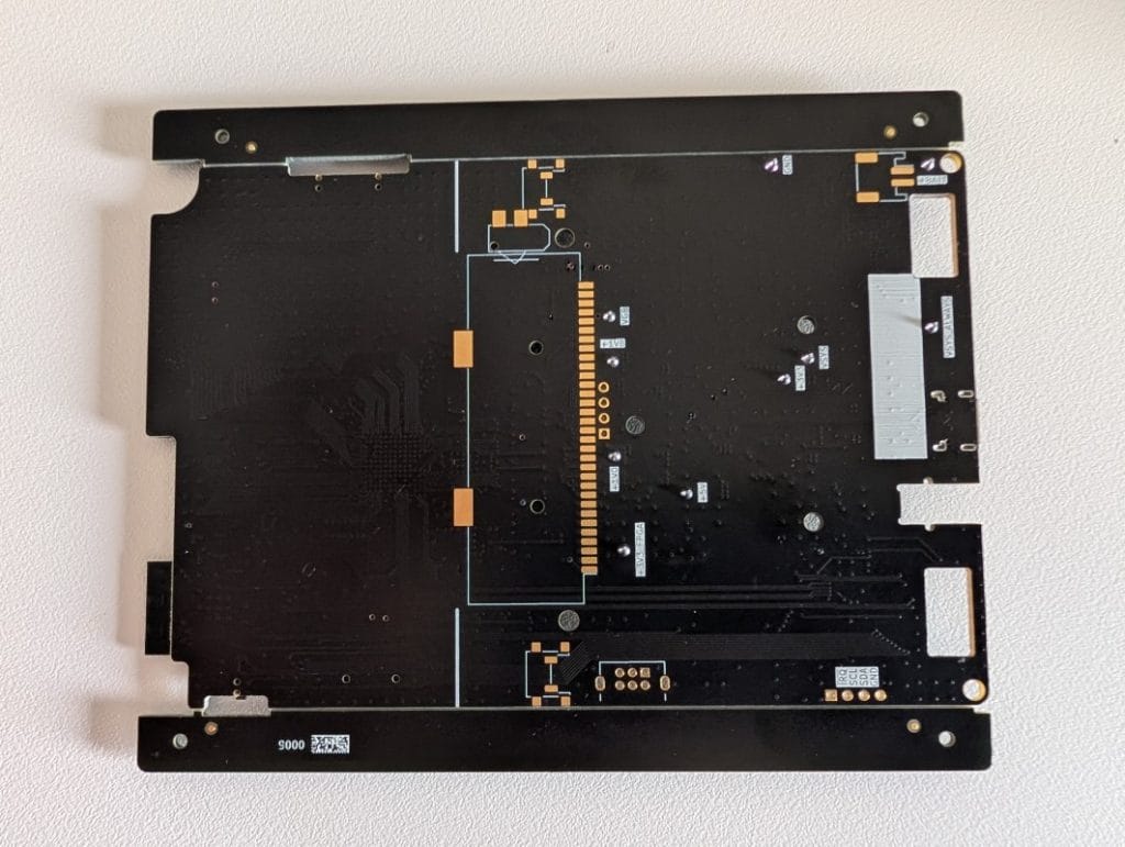
The PCB schematic is done in KiCad. You’ll need to install it too — I used KiCad 9.0, downloaded for free from kicad.org. But that alone isn’t enough. To place an order with a PCB manufacturer, you have to generate three types of files from the project: Gerbers (they describe each physical layer of the board), BOM (Bill of Materials, the component list with part numbers), and CPL (Component Placement List, coordinates and orientations for the pick‑and‑place machine).
There’s a plugin for each major PCB manufacturer. The catch — and this is the first place you’ll lose time — is that the JLCPCB plugin, called “Fabrication Toolkit”, does not show up in KiCad’s official repository. You have to install it manually: download the ZIP from github.com/bennymeg/JLC-Plugin-for-KiCad/releases and in Plugin and Content Manager use the “Install from File…” option. Make sure you look under the “Plugins” tab, not “Fabrication Plugins” — I wasted a few minutes before I figured that out.
Once it’s installed, open pcb/handheld_rev2/handheld.kicad_pro, go to PCB Editor → Tools → External Plugins → Fabrication Toolkit and hit Generate. The plugin outputs three files: handheld.zip (Gerbers), bom.csv, and positions.csv. These are the three things you upload to JLCPCB.
How a PCB order at JLCPCB actually works
I chose JLCPCB because the project and component list were designed around this manufacturer. I took the shortest path.
A PCB order isn’t like buying a product off a shelf. The board has to be built from your plans, the files are checked, and quite often you’ll get questions if something isn’t clear. JLCPCB were very responsive — they emailed all their questions and replied quickly.
I also chose to source the PCB components from them, mainly because they can solder them professionally. I don’t have BGA or fine‑pitch SMD soldering gear at home. In short: without a reflow oven, you can’t do much with a board that has a BGA‑packaged FPGA.
What you must set manually — the site can’t read it from the Gerbers
When you place the order, a few options have to be selected manually — the site doesn’t auto‑detect them:
- The Game Bub design uses 6 layers — you must choose the “High Precision PCB” option, not the standard 2‑layer variant.
- Surface finish: ENIG (Gold) — mandatory. Without ENIG you won’t reliably solder the FPGA’s BGA.
- Board dimensions: 90.1mm × 135mm — entered manually.
- Quantity: 5 (the standard minimum for assembly).
For shipping: the lightning‑fast option (2–3 days) is noticeably more expensive than the standard one (5–6 days). If you’re not in a rush, the standard option is perfectly reasonable.
The “Parts Selection by JLCPCB” flow — the first thing that will surprise you
JLCPCB doesn’t show you the final price as soon as you submit the order. If you want them to assemble the boards with components from their stock, the flow looks roughly like this:
- You pay a service fee for them to search for components in the LCSC stock.
- You wait 1–2 days.
- You receive an email with a report: what they found, what they didn’t, what substitutions they propose.
- You reply with your confirmations.
- Only now do you get the final price and pay the rest (PCB + assembly + components).
The surprise is that you pay an initial fee without seeing the full cost upfront, and the order doesn’t show up in your cart in the usual way after payment — it stays in a sort of stand‑by until they come back with the report. If you expect a classic e‑commerce flow (add to cart → pay → receive goods), this is different.
Clarifications with JLCPCB: questions you’ll probably answer too
There were a few rounds of emails. I’ll summarize them, because anyone doing the same project will get almost identical questions.
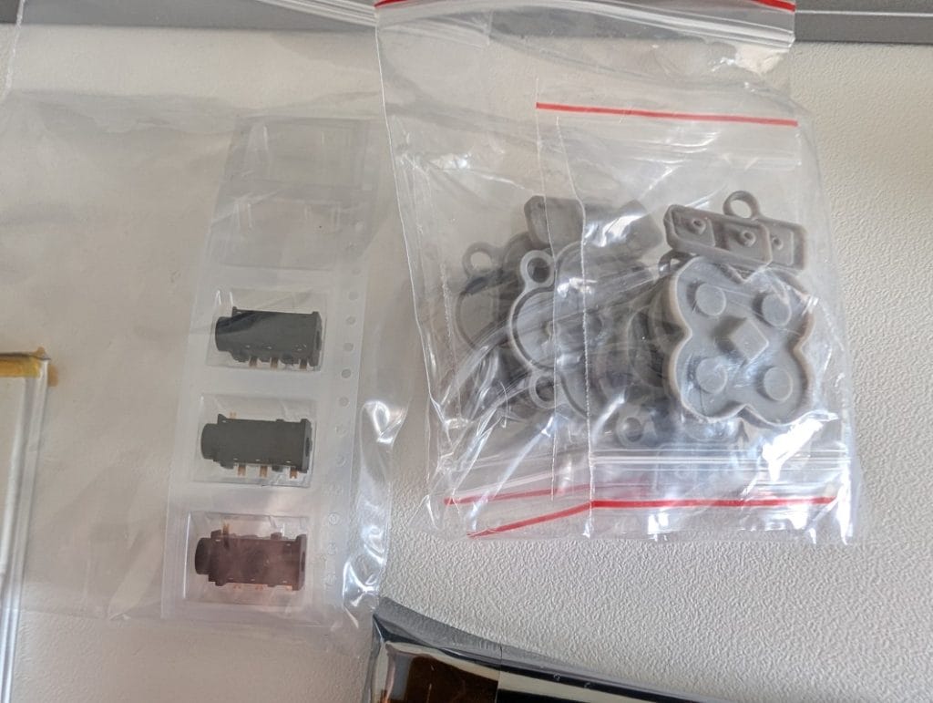
Designator mismatch: they asked about four pins in the schematic — JP1301, TP401, TP402, J1501 — that didn’t have a component in the BOM. These are a solder jumper, test points, and the vibration motor, all meant to be installed manually. I chose the “ignore and continue” option.
Proposed substitutions for components with limited stock — I accepted them after checking the datasheets:
- Tactile buttons SW1601–SW1608 → GT-TC155C-H0060-L50
- IMU LSM6DS3TR-C → LSM6DSDTR (functionally equivalent)
- IO expander TCA9535 → TCA9555PWR (UMW version)
- Logic shifters U1901–U2004 → SN74LVC1T45DCKR
- Test points → RH-5000
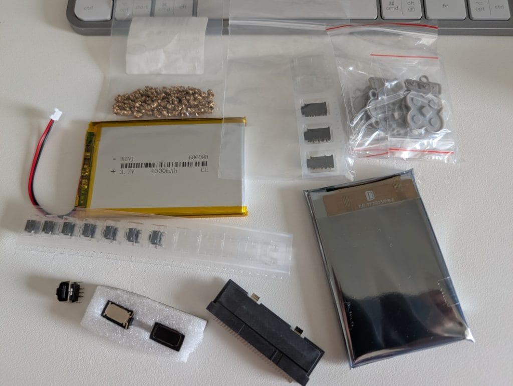
Unavailable components: the headphone jack SJ-43614-SMT-TR and the speakers CMS-160903-18S-X8. For the jack: option A, solder it manually. For the speakers: different supplier.
Missing components: AliExpress, Mouser, buydisplay
The remaining components are split between AliExpress and big distributors like Mouser or Farnell. AliExpress is reasonably fast in terms of delivery. Mouser and Farnell are quicker, but they use premium services only (UPS Express, DHL Express), and shipping prices match. For a hobby project, if you’re not in a hurry, AliExpress is perfectly acceptable.
To be soldered manually on the board:
- 3.5mm headphone jack SJ-43614-SMT
- GBA cartridge slot (search for “GBA cartridge socket”)
- 10mm coin‑type vibration motor
- GBA link port (optional)
- PMOD connector (optional, experimental)
- Shoulder buttons PTS645VN13SMTR92LFS
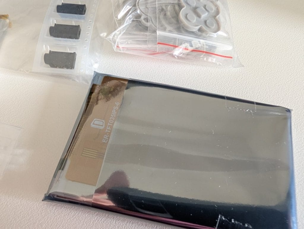
External components (not on the PCB):
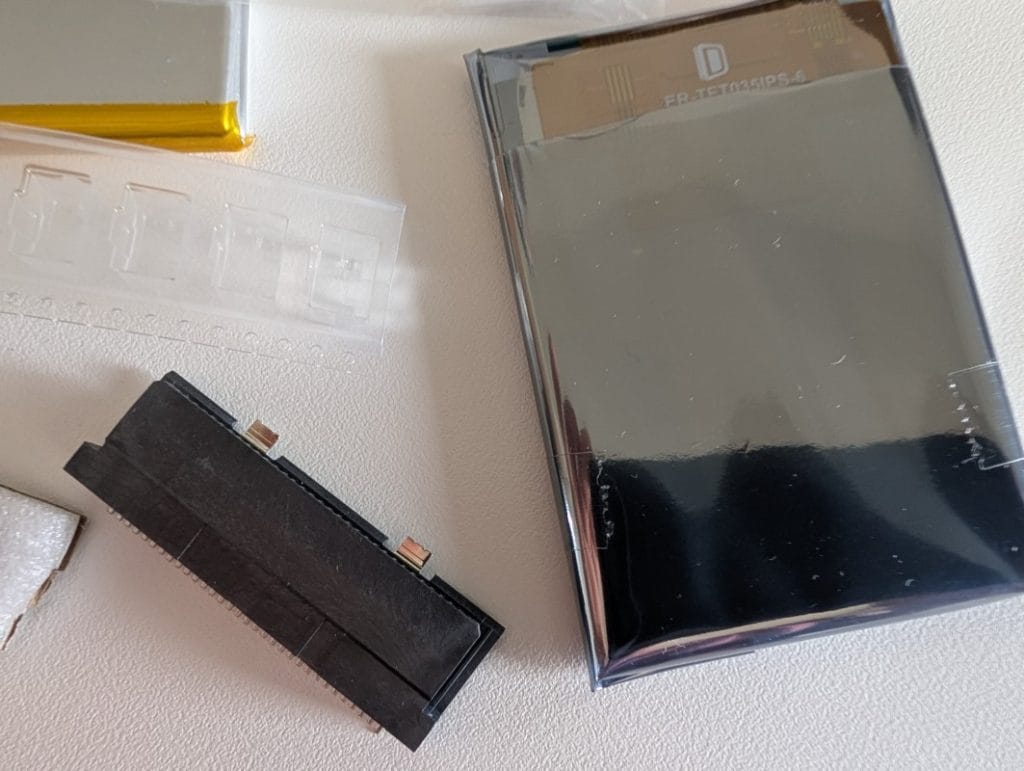
LCD display: ER-TFT035IPS-6 from buydisplay.com. Options when ordering: no touch panel, with 50‑pin FPC connector. If you run into terms like ZIF, ZIP, FPC, or FCC — in this context they all refer to the same type of flat‑flex connector.
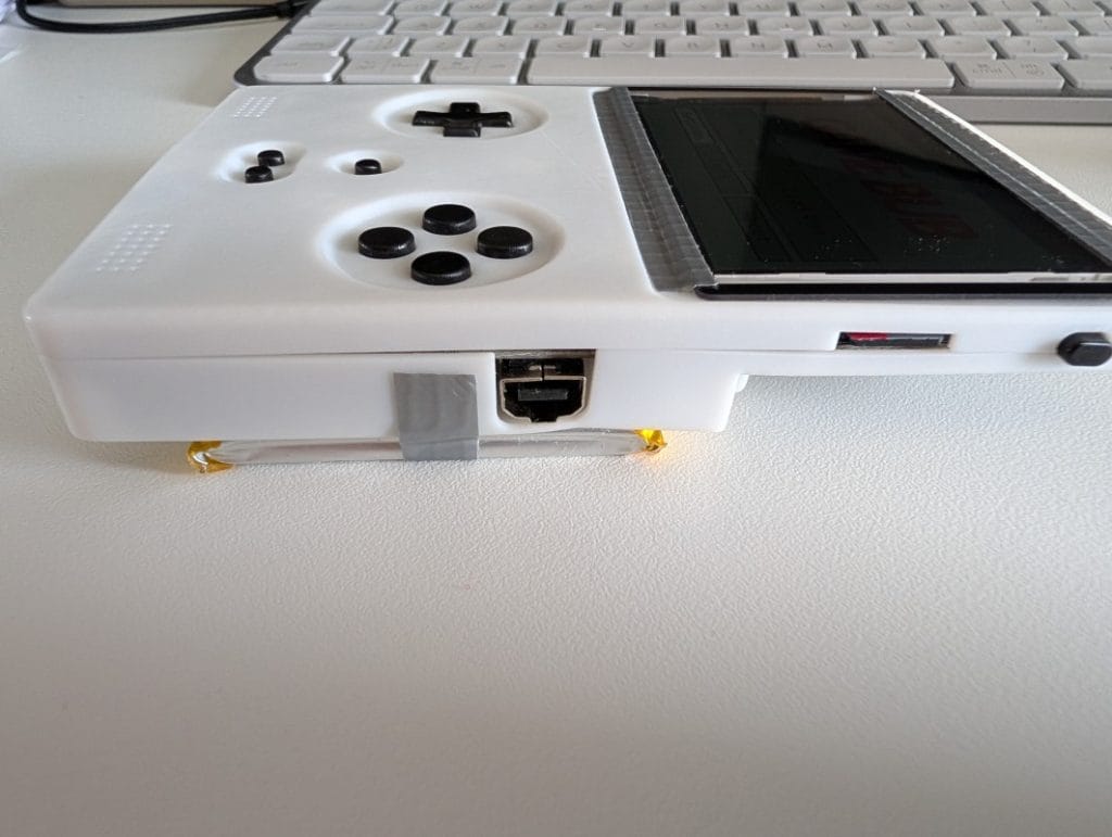
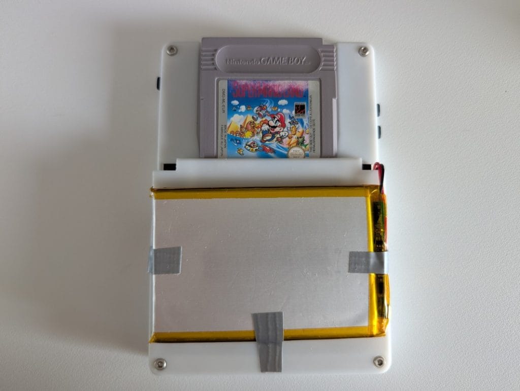
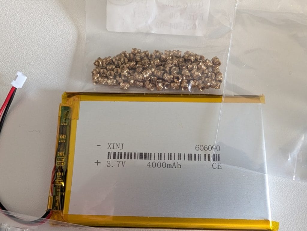
LiPo battery 755068, 3.7V, JST‑PH connector. Capacity 3000–4000 mAh depending on what you find. The 755068 code means 7.5mm thick × 50mm wide × 68mm long.
Speakers CMS-160903-18S-X8 — sourced from Mouser. They’re not soldered; they’re pressed against the PCB contacts when you assemble everything into the 3D‑printed shell.
Battery warning: some Chinese manufacturers mount the JST‑PH connector with reversed polarity compared to the commercial standard. Before plugging it into the PCB, always check with a multimeter. If you connect it backwards, you’ll fry the board.
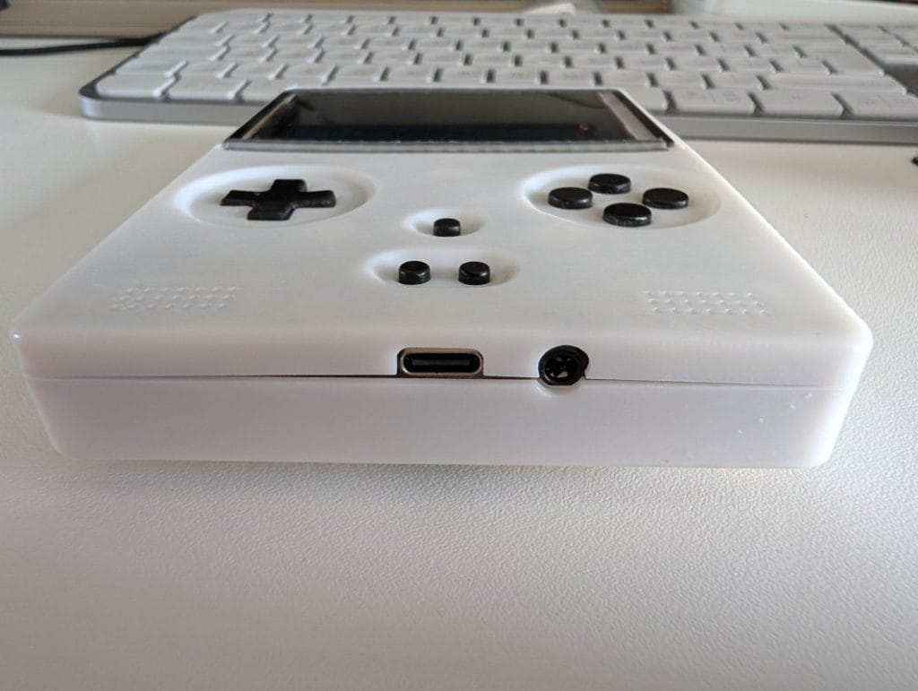
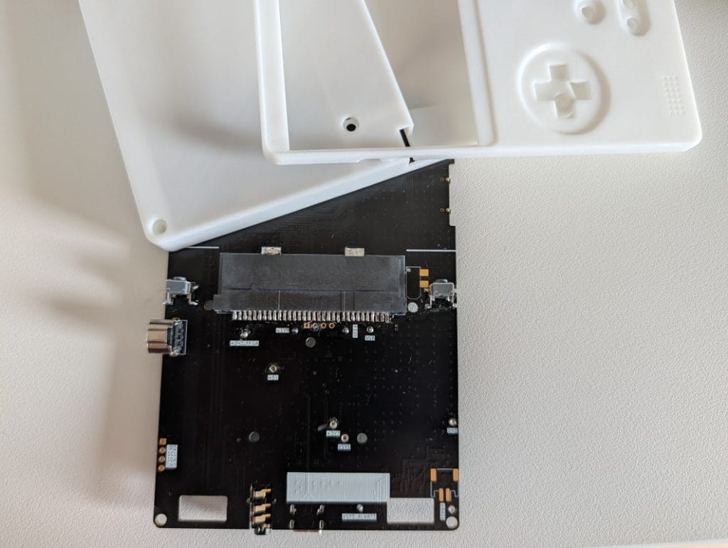
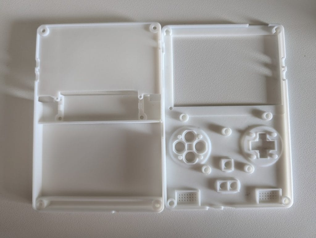
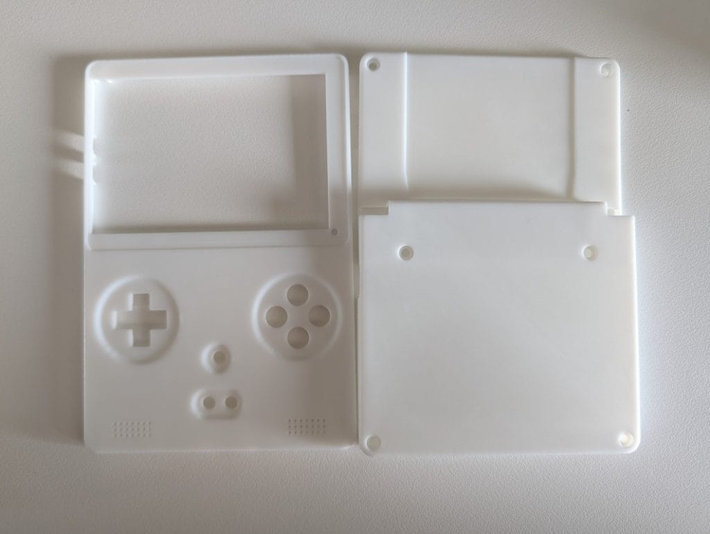
3D‑printed shell via JLC3DP
The STL files are in the project under 3d/handheld_rev2/: Front, Rear, DpadButton, FaceButtonArray, ExtButtonArray, SideButtonArray, ShoulderButtonArray.
JLC3DP (JLCPCB’s 3D printing service) was the obvious choice, but note: you can’t put the shell in the same cart as the PCBA. They’re two separate orders, with separate shipping.
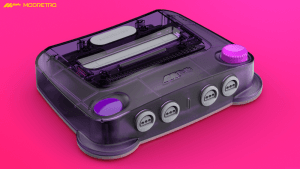
Material: I chose 9600 Resin (SLA), Matte White. The community almost always goes for the transparent resin (8001 Resin) so the PCB is visible through the shell — it looks great in photos. But the transparent one is more fragile and considerably more expensive. For a practical prototype, I went with the solid, cheaper option. If you want the internet‑friendly showpiece others build with sponsor money, pick the transparent one.
The option to have different button colors (yellow, red, like the original Game Boy) pushes the price up quite a bit. I didn’t think it was worth it, especially since I wasn’t even sure I’d manage to finish the project.
Screen protection glass — the unresolved chapter
The original author ordered custom tempered glass: 0.7mm thick, black silkscreen on the back, 3M adhesive. At low quantities it gets pretty expensive.
The alternative I explored was using glass from a Nintendo DSi. It looks different and doesn’t fit perfectly on the 3D‑printed shell, but it works for experiments. Ideally, I’d modify the front shell STL to match this glass — something for the future.
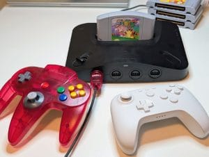
About 3–4 weeks after the first order, I had the PCB and most of the components in front of me.
A few important things to know about ordering:
You can’t order PCBs one by one. Most manufacturers have a minimum of 5 pieces. And you’ll almost inevitably mess up at least one AliExpress order, especially for components without a clear part number. In my case: the batteries were too big and didn’t fit in the shell, the metal pins for the buttons were too short, and the springs for the L and R buttons as well. Maybe I messed up the order, maybe I just wasn’t careful enough. Either way, it’s part of the process.
First power‑on: firmware, ESP32, and FPGA
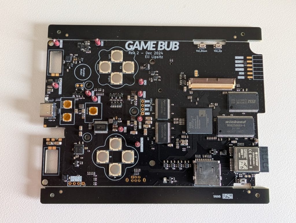
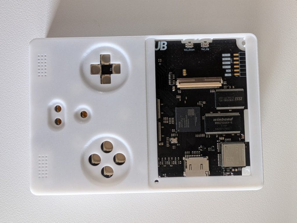
The PCB arrived from JLCPCB assembled, with all SMD components soldered. The next step was to put software on it. Without firmware, the board does nothing.
The first test was simple: I connected the LCD flex cable and a USB‑C cable. The green status LED lit up — the board was getting power, so the hardware side looked fine. Nothing on the screen, because the ESP32 didn’t have any program on it yet.
FPGA and microSD
The Game Bub has two programmable components: an Artix‑7 FPGA, which emulates the Game Boy and GBA in hardware, and an ESP32‑S3, which handles the UI, SD card, and display. For the FPGA, the project’s author has already published pre‑compiled bitstreams in the v0.1 GitHub release: boot.bit.gz, gameboy.bit.gz, gba.bit.gz. You don’t have to compile anything.
I formatted a 128GB card as FAT32 using Rufus, created a system/ folder, and dropped in those three files plus the BIOS images: SameBoy boot ROMs for GB/GBC and the open‑source Cult-of-GBA BIOS for GBA, renamed according to the project documentation.
ESP32 firmware: wrestling with the toolchain
The firmware is written in Rust and uses Espressif’s ESP‑IDF. On Windows I immediately hit a classic problem: the build path exceeded the system’s 260‑character limit. I switched to macOS, where everything runs natively.
Toolchain installation:
bash
curl --proto '=https' --tlsv1.2 -sSf https://sh.rustup.rs | sh
cargo install espup && espup install
cargo install espflash
I also had to manually set a few environment variables so the build could find ESP‑IDF’s Python environment, after which compilation worked — it takes about 10–15 minutes the first time you run it:
bash
. ~/export-esp.sh
cargo run --release --features=rev2
Espflash automatically detects the USB port and flashes the firmware. The final step: the flash_nvs.py script writes the hardware revision and board serial number into NVS — without this, the firmware refuses to boot.
bash
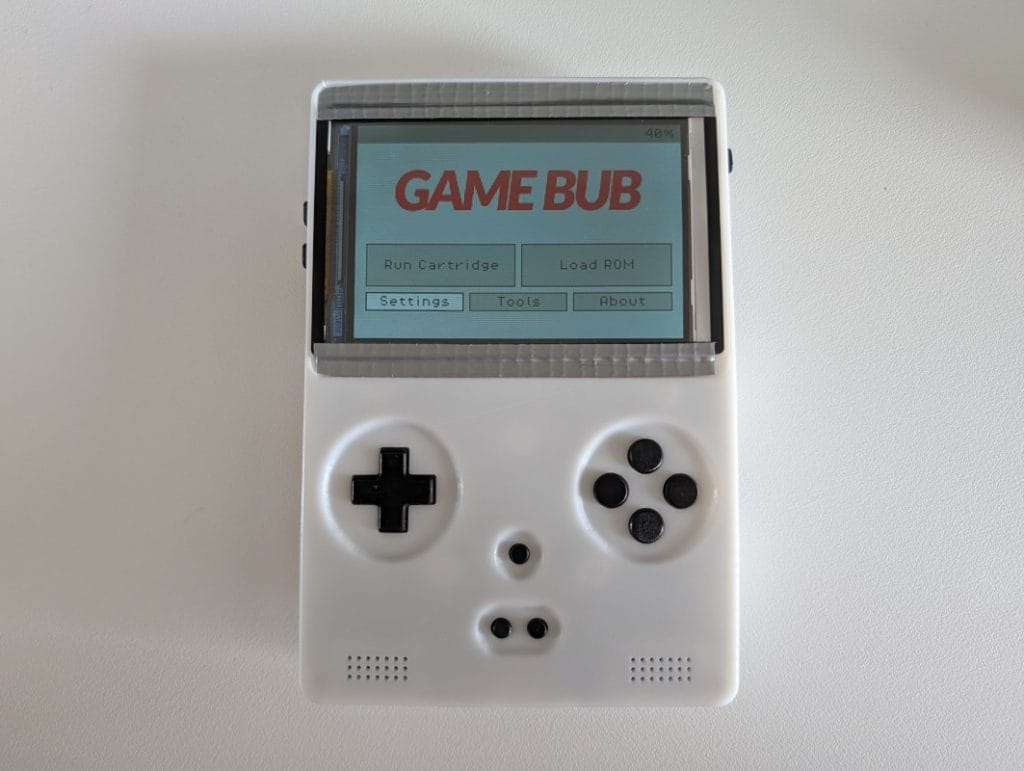
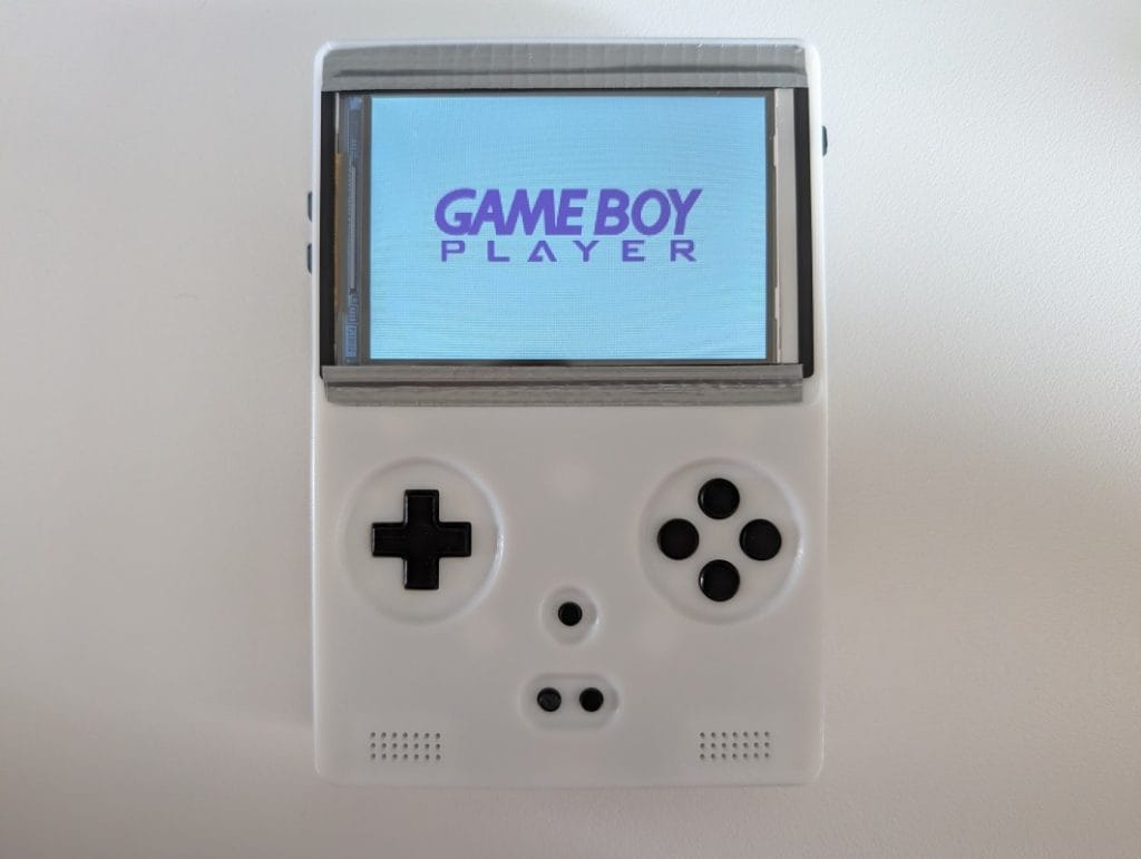
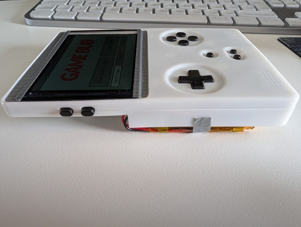
python3 flash_nvs.py --serial 0001 --revision 2Card in the slot, Power pressed — the Game Bub menu on screen. Boot animation, logo, main menu. The first working board, from a project started from scratch, one I wasn’t even sure I’d be able to see through.
The finished product: what stands out and what still needs polish
Let’s talk a bit about the product itself, even though mine isn’t truly final — as I mentioned, it really grabbed my interest and I started modifying it, especially the firmware, FPGA, and software.
What the original developer pulled off, essentially as a one‑man show, can largely rival products built by companies with dedicated teams and proper budgets. The FPGA implementation, the PCB design, and the Rust firmware built from scratch, plus compatibility with original GB, GBC, and GBA cartridges and ROMs from an SD card — it’s genuinely impressive.
On the other hand, I’d classify it as a device that, when you hold it, feels like a very solid hobby project rather than a polished retail product. The state of the GitHub project explains that feeling: in many areas it still needs refinement, and that work hasn’t happened in the public repo. It’s somewhat understandable, because the original author moved toward a commercial direction via crowdfunding, and it’s normal to keep a few aces up his sleeve there.
The areas I identified as needing further evolution:
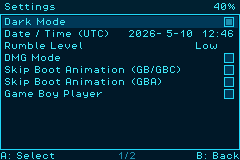
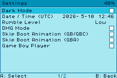
The firmware, in its original form, only covers the basics. There are features present in the menu but not implemented in code, and bugs that show up in specific situations — long ROM lists would trigger a panic crash because they exceeded available memory. Dark Mode is unimplemented, Rumble has no way to adjust vibration motor power levels. Beyond that, I felt there were other missing pieces, which I added in my modified firmware; you can spot some of them in the gallery images.
The PCB, in my view, could also use some refinement. The power and volume buttons feel fragile for heavy use. I’d replace the volume buttons with a classic radio‑style wheel, far more reliable over time. The power button, which will be one of the most stressed controls on the console, I’d swap for a sturdier through‑hole part instead of SMD — I say this from experience, because my power button broke during assembly. The 3D‑printed shell naturally has tolerances that mean the buttons don’t sit perfectly on the SMD components underneath.
Still on the shell: while it’s convenient and fast as a solution, the material tends to warp more than an injection‑molded case, which means the two halves — front and back — don’t close together perfectly.
Even so, the device remains exceptional for something built by a single person. If you’re into electronics, it’s contagious. Since I started building it, I’ve been hooked enough to add new firmware features and extend compatibility to other consoles on the same hardware. At some point, when time allows, I’ll push all my changes back to GitHub so others can benefit from them.
Build costs vs. ready‑made: let’s talk money
On the Crowd Supply crowdfunding page, you can order a Game Bub for $269 plus $18 shipping. That price is probably before tax, so in Europe you need to add roughly 20%, which brings the total to around $344.
My costs, for everything I ordered, including shipping and import taxes where applicable:
- AliExpress components: €31.51
- JLCPCB (PCB, PCB components, 3D shell plus fees): €156
- Mouser components: €12.64
Total: roughly €200, or about $215–220.
Of course, the crowdfunding price benefits from volume discounts — my per‑component cost is higher than when you’re building a few hundred units. The difference might be around 20%. And I can add another 5–10% margin for error and optimization on my side.
If you want the final product, clearly more polished and refined than what’s on GitHub, ready to use straight out of the box — the Crowd Supply option is for you.
If you’re passionate, if you want the learning curve and to walk away with knowledge you can reuse in future projects, if you want to be proud of your skills — then the GitHub project is the one to pick. The journey from placing orders to holding a working device in your hands will be far more satisfying than just grabbing it off a shelf.
If this is your first project of this kind, honestly, the savings alone probably aren’t worth it per se. You’ll put in at least 4 weeks of work to save about a hundred dollars. But you’ll go through the whole process: KiCad, BOM, PCBA, manual assembly, firmware setup. You’ll learn how to build a board with an FPGA and BGA with your own hands. And you might even end up contributing back to the community. That part can’t be measured.
P.S. I’m sure I’ve forgotten some details about the project — that’s normal, I spent several weeks both building it and working on additional development. If you start the project and have questions, write in the comments section and I’ll reply.
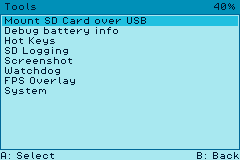
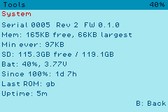
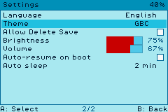
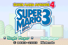
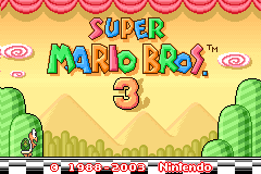
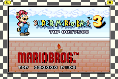
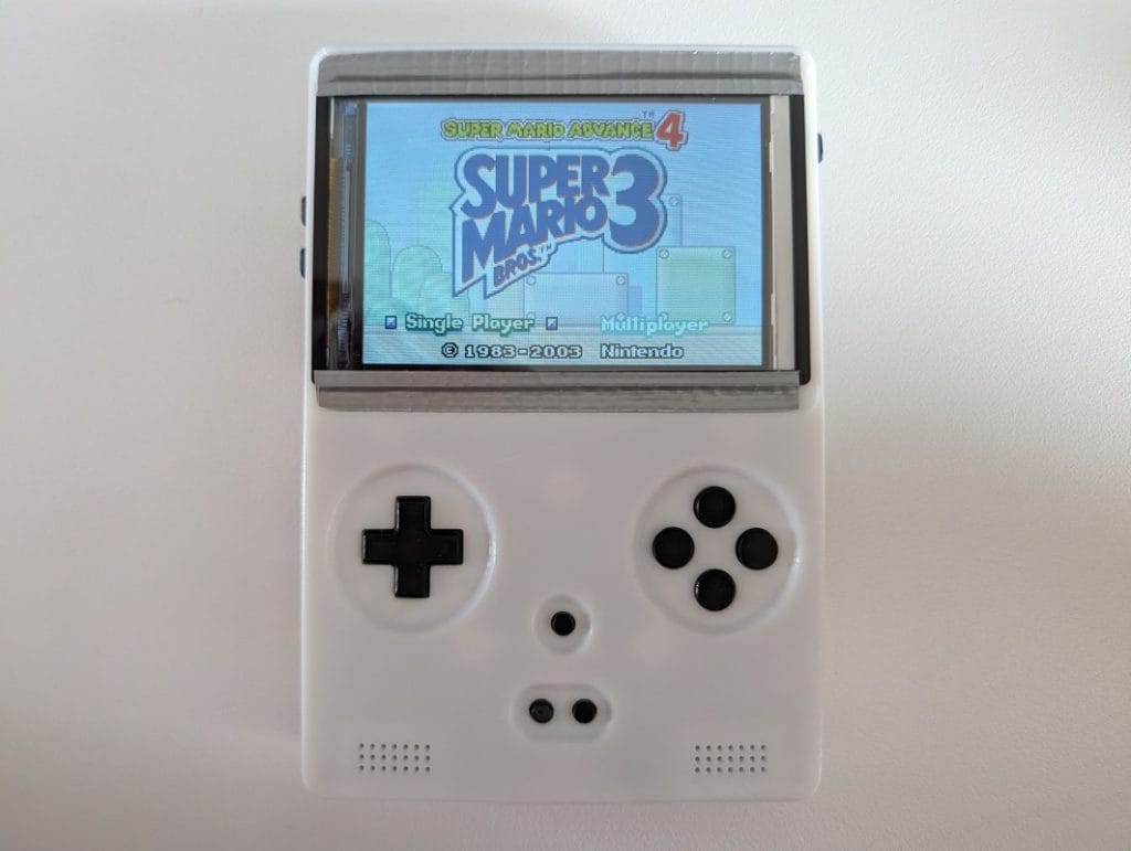
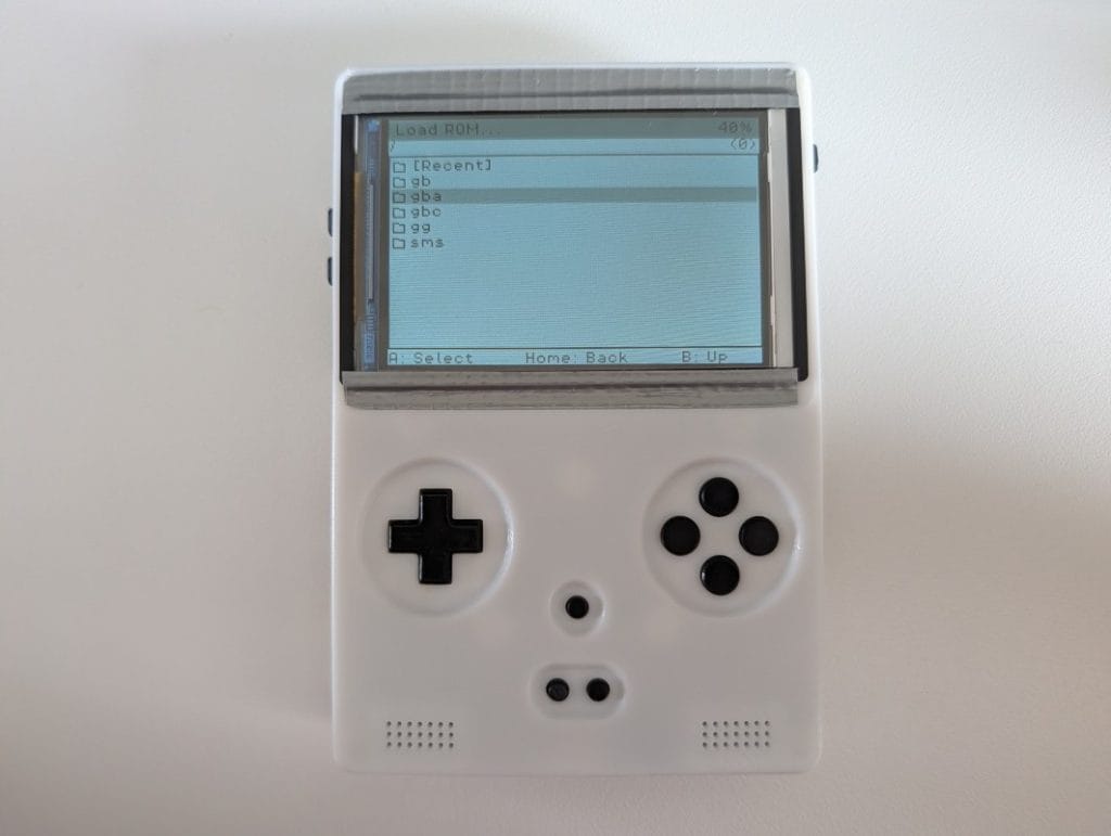
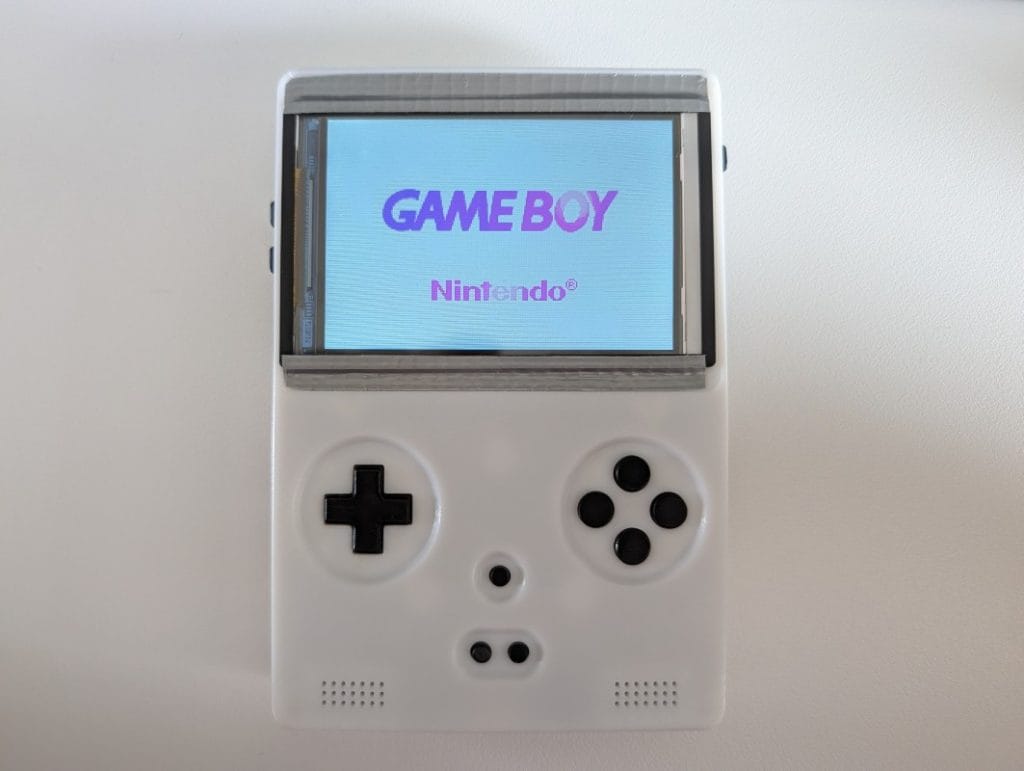
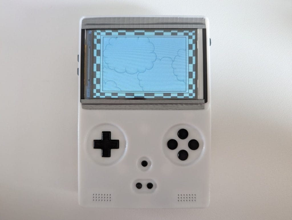
Gallery with screenshots from the menu and in-game
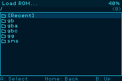
(screenshot functionality is one of the features I implemented in the custom firmware)
Project build log photos

Articles selected automatically based on the current article. Model: gpt-5